Global supply chains have felt the impact of the pandemic for quite some time and continue to face challenges navigating the disruption of production lines even as more regions of the world and business centers gradually re-open and bring more personnel back on-site. The biggest challenge that will remain for the foreseeable future is the shortage of semiconductors, and the signs have been there for months.
Last December, Volkswagen said that semiconductor bottlenecks meant it would produce 100,000 fewer cars in the first quarter of 2021, as its parts makers were unable to secure supplies. Nissan, Renault, Daimler and General Motors are also struggling with the shortage, which may lead to production being reduced by as much as 20% per week.
In February, the unexpected snowstorms that hit Texas also significantly impacted the supply chains supporting semiconductor production, causing even more delays.
New manufacturing lines are required for semiconductor fabrication plants, otherwise known as fabs, to increase capacity. A key challenge has been that the semiconductor capital equipment manufacturers helping to enable fabs in meeting the demand are unable to pivot their own product development cycles and production to meet the increased need. They are challenged by their reliance on traditional manufacturing technologies, however integrating additive manufacturing (AM) can be a game-changer.
Additive manufacturing delivers immediate benefits to capital equipment manufacturers
Traditional manufacturing workflows are hampered by several limitations when trying to quickly ramp up production. Additive manufacturing, also known as 3D printing, removes these limitations, enabling freedom of design and a seamless transition from prototyping to low-volume production of bespoke parts. Three applications of AM, in particular, have demonstrated advantages to capital equipment manufacturers.
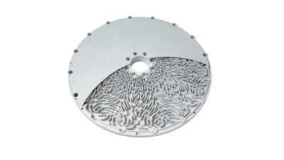
Wafer table thermal management. Better thermal management of critical semiconductor equipment components, such as wafer tables, can improve semiconductor equipment accuracy by 1–2 nm and simultaneously improve speed and throughput. An increased machine speed and uptime leads to more wafers processed and higher overall lifecycle value.
During lithography, keeping temperatures within milliKelvin (mK) ranges is critical as any system disturbance has an impact. Through design for additive manufacturing (DfAM), it’s possible to optimize internal cooling channels and surface patterns, thus dramatically improving surface temperatures and thermal gradients while reducing time constants. A large semiconductor capital equipment manufacturer using AM to produce their wafer tables realized an 83% decrease in ΔT (13.8 to 2.3 mK), and a 5-time reduction in time to wafer stabilization.
Another benefit of using AM to produce wafer tables is structural optimization and tables with reduced part counts and assemblies. Producing parts using traditional technologies relies on brazing to join parts together, which is a lengthy, low-yield process with a 50% rejection rate. Replacing multipart assemblies with monolithic additively manufactured parts increases reliability, improves manufacturing yield and reduces labor costs.
Manifold fluid flow optimization. Using traditional manufacturing processes to produce complex fluid manifolds results in large, heavy parts that have non-optimal fluid flow due to abrupt transitions between components, and channels with sharp angles that lead to disturbance, pressure drops, stagnant zones and leakage.
When AM is employed to produce these same manifolds, engineers can optimize their designs to reduce pressure drop, mechanical disturbances and vibration. A 90% reduction in flow-induced disturbance forces reduces system vibration and realizes a 1–2 nm accuracy improvement.
Structural optimization and advanced flexures. AM gives designers the flexibility to optimize the structural topology of your part (i.e. lightweighting) with a suite of high-strength metal alloys. These designs can more precisely meet the performance requirements of semiconductor capital equipment, improve the strength-to-weight ratio and deliver a faster time to market. Lightweighting semiconductor components and advanced motion mechanisms reduces inertia and improves lithography and wafer processing machine speed and uptime, leading to more wafers processed. In one example, a semiconductor capital equipment manufacturer was able to employ AM to achieve greater than 50% weight reduction in flexures, 23% higher resonant frequency and reduced system vibration.
Additive manufacturing can open new doors
AM – specifically direct metal printing – is a recognized, validated technology in the semiconductor capital equipment industry. The pressures within the market for optimization, the demand for more equipment, and the production barriers are requiring a rapid movement toward additive.
From a lithography perspective, there is currently a large volume of equipment already being used in production to create chips using a ~14nm process. A likely scenario is that AM will significantly enable newer machines that are either shipping today or will be shipping in the next 1-2 years. With this runway, there is ample time for component and system level redesigns, which will increase productivity and quality. Additionally, the manufacturers will still have enough control over those systems to rigorously test and prove performance gains.
Outside of lithography, there are dozens of other applications in the process chain such as polishing, light sources and etching, sorting and even metrology. AM is allowing semiconductor capital equipment manufacturers to rethink what is possible and push the boundaries. There is a tremendous opportunity for AM to help overcome the semiconductor shortage, and once again, strengthen supply chains.