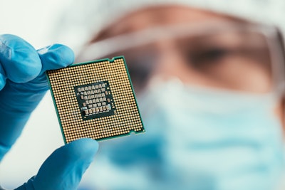
Advanced packaging techniques play an increasingly critical role in enhancing the functionality of components. This enables them to meet the soaring demand for semiconductors to power today’s emerging technology innovations. These technologies require efficient processing of vast data sets and therefore are best served by high-performance, low-power chips. Advanced packaging eliminates bottlenecks and reduces costs by stacking chips in three dimensions and establishing direct connections between them and in transitional integrated circuits. As chipmakers race to gain a competitive edge, advanced packaging is emerging as the next battleground for major players like TSMC, Samsung and Intel, to capitalize on their innovations and attract premium customers.
The Growing Demand for Advanced Packaging
Demand for advanced packaging is rapidly increasing, driven by several key factors. One of these primary catalysts is the rising complexity of semiconductor designs. As technologies evolve, chips are required to perform more functions in smaller form factors, necessitating intricate packaging solutions that can accommodate these advanced designs.
Additionally, the performance requirements in new applications—such as high-speed computing, AI, and IoT—are pushing the boundaries of what traditional packaging methods can achieve. These applications demand not only greater processing power but also improved energy efficiency and thermal management, further highlighting the need for innovative packaging solutions that can meet these stringent performance criteria. Consequently, the semiconductor industry is not just adopting but increasingly relying on advanced packaging as a critical enabler for the functionality, performance and efficiency demanded by today’s most cutting-edge technologies.
Cutting-Edge Innovations in Semiconductor Packaging
Currently TSMC, Samsung and Intel dominate the realm of advanced packaging. These industry leaders are not only at the forefront of node advancements, with ambitious plans for sub-2nm production schedules in the coming years, but they are also fiercely competing to secure the top position in advanced packaging technologies. TSMC, which began investing in advanced packaging nearly a decade ago, has patented an impressive nearly 3,000 technologies in this domain. Samsung closely follows with around 2,400 patents, while Intel holds third place with 1,400.
In 2022, Samsung significantly boosted its efforts by establishing a dedicated team to innovate in packaging processes. Their initiative, Samsung Advanced Interconnection Technology (SAINT), aims to revolutionize chip integration by connecting different types of chips to function cohesively as a single unit. Unlike traditional horizontal placements, SAINT employs a distinctive 3D packaging approach that vertically stacks chips, optimizing space and performance. Samsung has achieved successful technical verification for various iterations of its SAINT technology, particularly with its SRAM variant, SAINT-S, and anticipates finalizing its DRAM version, SAINT-D. This latter technology focuses on stacking DRAM directly atop processors, including CPUs and GPUs, enhancing data storage and processing efficiency.
Meanwhile, TSMC has made significant strides by opening its first all-in-one advanced packaging and testing facility. This facility is dedicated to producing its system-on-integrated-chip (SoIC) and 3DFabric technologies tailored for artificial intelligence applications and data centers. During the AI surge of 2023, propelled by the popularity of tools like ChatGPT, TSMC's advanced packaging process became essential for Nvidia’s sought-after GPU product lineup. Last year, TSMC faced immense pressure to meet the rising demand for AI-capable components from Nvidia, AMD, and Amazon, leading to a 30% increase in equipment orders for its chip-on-wafer-on-substrate (CoWoS) technology. This high-density packaging solution was essential for TSMC’s advanced chips, enhancing functional density, performance, and power efficiency while minimizing PCB size and thickness.
How Advanced Packaging Fuels the Future of Technology
As the technological landscape continues to evolve at a breakneck pace across industries, the importance of advanced packaging in semiconductor manufacturing cannot be overstated. With its ability to enhance power efficiency, increase processing speed, and address the complex demands of emerging applications like AI, 5G and autonomous vehicles, advanced packaging stands at the forefront of innovation. Industry leaders like TSMC, Samsung and Intel are already reaping the benefits of significant investments in this area, highlighting the urgent need for other stakeholders to follow suit.
Advanced packaging plays a vital role in addressing the unique challenges faced by emerging sectors. For instance, real-time data processing is essential for artificial intelligence applications, where delays can compromise functionality. In the realm of 5G communication, advanced packaging helps meet the high bandwidth and low latency demands necessary for seamless connectivity. Similarly, in the development of autonomous vehicles, advanced packaging ensures safety and reliability by facilitating the integration of multiple sensors and processing units that must operate flawlessly in real-time. Advanced packaging not only enhances the capabilities of individual components but also supports the robust demands of these cutting-edge technologies, paving the way for innovations that could reshape various industries.
To remain competitive and drive future advancements, it is imperative for companies across the semiconductor supply chain—manufacturers, suppliers and technology developers—to invest in advanced packaging innovations. By prioritizing research and development in this critical field, industry players can not only meet the growing demands of modern technology but also unlock new opportunities for growth and collaboration.


